Focused Ion Beam – Scanning Electron Microscope (Helios 600 - Dual Beam)
Located in EMSL | Stewarded by Odeta Qafoku

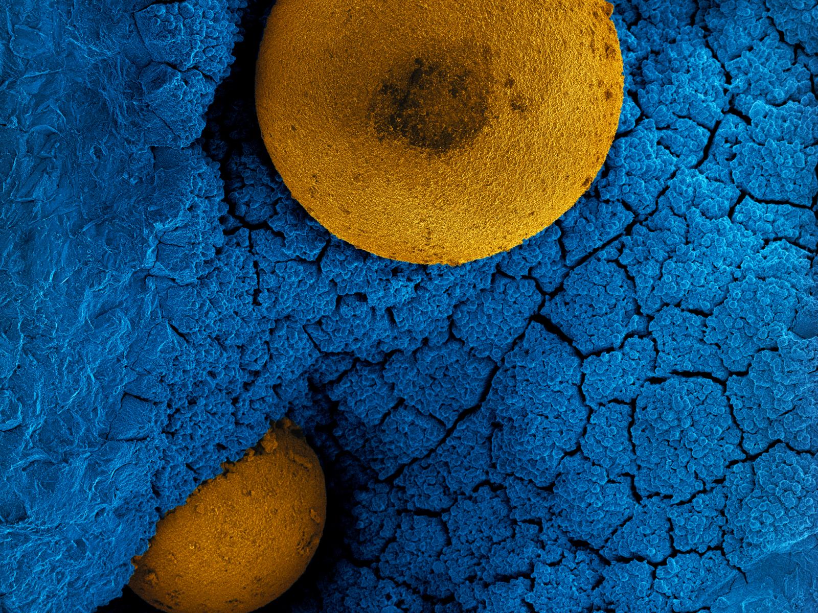
Basalt rocks convert CO2 into calcium carbonate nodules. Scientist at PNNL are studying capture of CO2 by subsurface basaltic rocks, to mitigate the increasing CO2 levels in atmosphere.
Odeta Qafoku
Mission
The FEI Helios Nanolab DualBeam Focused Ion Beam/Scanning Electron Microscope (SEM), equipped with an energy dispersive X-ray spectroscopy detector (EDX), combines important high-resolution microscopy tools. This allows for integrating:
- highly valued imaging at nanoscale resolution,
- elemental analysis and characterization of materials at micron to submicron scale, and
- preparation of ultrathin samples and materials for other analysis—e.g, preparation of selected regions for transmission electron microscopy (TEM) and atomic probe tomography (APT).
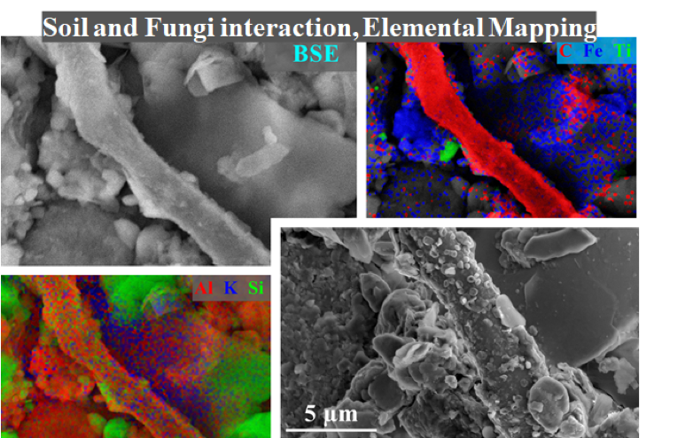
Functionally, the instrument includes high-resolution SEM imaging based on a field-emission-gun electron source and computer-controlled ion-beam micromachining based on a Ga liquid-metal ion source. The instrument is also equipped with EDX that utilizes an 80 mm2 silicon drift detector, characterized by high stability and accuracy given its large analytical area. The detector permits high-count rate mapping at low and high energies, can detect lighter elements with accuracy starting from Be, can perform chemical analysis on rough surfaces, and can identify phase composition for submicron particles.
Helios NanoLab provides rapid and detailed morphological analysis of micro to nanoscale particles and is equipped with Oxford multi-tasking software (AZtecLive and AZtecFeature) that enable real-time sample navigation based on sample chemistry and/or advanced particle analysis platform. Specifically, AztecLive collects live X-ray chemical data with real-time chemical feedback in an interactive way that allows for investigation of sample morphology and sample chemistry simultaneously. The AztecFeature automatically collects large EDX chemistry maps with rebuild and montage features that are based on higher resolution/smaller area maps.
Helios NanoLab allows for sample preparation by FIB for scanning/transmission electron microscopy (S/TEM) imaging or fabrication purposes, such as welding to a TEM sample grid without breaking the vacuum within the instrument. The samples prepared using FIB are analyzed by high resolution surface and bulk sensitive electron capabilities including APT, secondary ion mass spectrometry, and TEM.
Features
- Nanometer scale focused spot size
- Performs FIB/SEM, EDX, and S/TEM
- Real-time chemical feedback platform for accurate elemental maps
- Particle analysis and chemical map montage platform
- Immersion mode allows nanometer scale high resolution imaging
